Thin Film Technology
Thin Film Technology
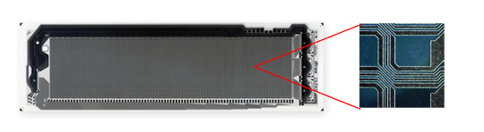
Enables high resolution pattern formation on glass substrate by aluminum thin-film
From small lot to high volume production by Noritake automated system and Quality control
Noritake performs fine pattern forming by utilizing aluminum spattering and photo process.
The patterns can be formed on glass substrate with high resolution.
Also available with Black layer pattern (Noritake original) to prevent reflection,Transparent Conductive Polymer (ITO polymer) formation as well.
Combination of thin and thick film patters brings new possibility to your products.
Noritake also specializes in high precision formation on large glass circuit board (maximum size: 500mm).
| Line Pitch | 40 μm min |
|---|---|
| Line Width | 15μm min |
| Line Color | Al Silver (Mirror), Black |
| Materials | Aluminum, ITO(Indium Tin Oxide), SiO2, etc. |
| Substrate Material | Glass, 0.7 to 5mm thickness |
| Application in VFD | Glass substrate circuit formation with combination of thick film multi-layer |
* Please inquire if you have higher requirements
-
Thin Film Technology
-
Thin Film Technology
-
-
Thick Film Technology
-
High precision Mounting Technology
-
Vacuum Technology
-
Embedding Soft and Hardware Technology