TECHNOLOGY
Thick Film Technology
Thick Film Technology
Thick-film high precision pattern formation to align with Thin Film patterns
Noritake Thick Film Technology enables high precision pattern formation aligned with Thin Film patterns.
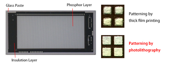
Photolithography can also pattern phosphors, insulators, etc. with even higher precision.
Wiring formation with high positional accuracy is possible up to 500x350mm.
| Photolithography | Dot Pitch | 325μm min. |
|---|---|---|
| Dot Size | □200μm min. | |
| Thick Film Printing | Line Pitch | 500μm min. |
| Line Width | 200μm min. | |
| VIA hole | 60×150μm min(Hex shape) | |
| Printing Material | Conductive materials – Silver.etc Black insulator, Transparent insulator Glass paste, etc. |
|
| Substrate Material | Glass, Ceramics, etc. | |
| Application in VFD | Display pattern, Insulation layer formation, etc. | |
* Please inquire if you have higher requirements
*the square “◻” symbol means both side members are the same length
-
Thin Film Technology
-
Thick Film Technology
-
Thick Film Technology
-
-
High precision Mounting Technology
-
Vacuum Technology
-
Embedding Soft and Hardware Technology