Power Supply Sequence
Power Supply Sequence
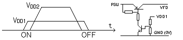
Fig. 9 - Power Supply Sequence and Safety Circuit
While the display power is being supplied, if the logic supply voltage "VDD1" is floating, or is kept at less than "+4.5V", the driver chips may be PERMANENTLY DESTROYED. Special care must be taken with the power supply SEQUENCE when the system is switched on or off. Please FOLLOW the sequence in Fig. 9 when switching the power on and off.
"VDD1" and "VDD2" should be ON at the same time,
or "VDD2" should be ON after "VDD1" is ON.
Power Off:
"VDD1" and "VDD2" should be OFF at the same time,
or "VDD1" should be OFF after "VDD2" is OFF.
In other words, this means "NEVER apply VDD2 without VDD1".
This can be achieved by putting a suitable PNP transistor in the VDD2 supply after any capacitors and controlling it's turn on from the presence of 5V as shown in the circuit of Fig. 9.
There is no specific restriction on the on/off timing of the filament power, it may take one second for the filament to raise its temperature to the optimum value after the filament voltage "Ef" is turned on. Before this time period is reached, no segments can be illuminated.
Chip in Glass VFD (BD-VFD)
-
Operation and Structure
-
Power Supply
-
CIG VFD Interfacing
-
Control Procedure
-
Custom Design Guidance
-
Others