Overlapping Grid Scan for Graphic Displays
Overlapping Grid Scan for Graphic Displays
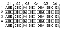
Fig.18 4 Way Anode Separation
Each grid has 2 columns of anodes.
There are 4 sets of anodes ABCD
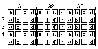
Fig.19 8 way Anode Separation
Each grid has 4 columns of anodes.
There are 8 sets of anodes ABCDEFGH
t graphic dot matrix CIG VFDs require a particular scan procedure known as 'overlapping grid scan'. This occurs when the space between anodes is small and it is necessary to turn on 2 adjacent grids at the same time in order to produce an even electron flow and consequently an even illumination of the anodes at the center of the adjacent grids.
There are several combinations of anode that can be used. Fig 18 and Fig 19 show the 4 way and 8 way schemes.
In the 4 way scheme, when Grid 1 and 2 are ON, anodes B+C are active. Then, when Grid 2 and 3 are ON, anodes D+A are active.
ouble Anode Driver Scheme
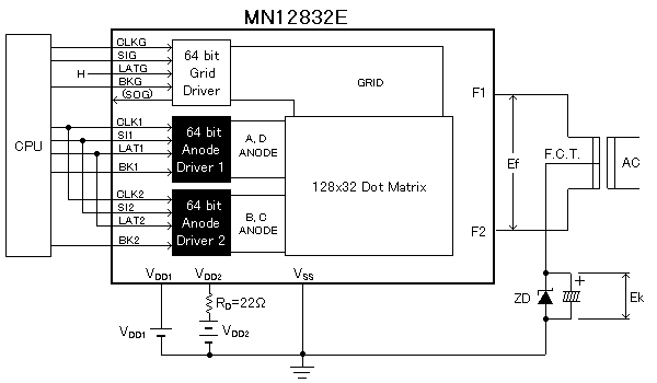
Fig.20 Block Diagram for MN12832E Double Anode Driver
To simplify the user circuit, the A+D and B+C anodes are controlled by two separated anode drivers with their serial data, clock and latch signals common and their blanking inputs BK1 and BK2 separately controlled to act as chip select (/CS) inputs. Although identical anode data is sent to both drivers, only the desired A+D or B+C driver is selected according to the pair of adjacent grids which are active. This sequence can be identified in the table below.
| Time Slot | Grids to be selected | Grid Driver Outputs | Blanking control | Anode data turned on | |||||||||||
|---|---|---|---|---|---|---|---|---|---|---|---|---|---|---|---|
| G1 | G2 | G3 | G4 | G5 | ....... | G60 | G61 | G62 | G63 | G64 | BK1 | BK2 | SI1/SI2 | ||
| T64 | G63+G64 | L | L | L | L | L | L | L | L | L | H | H | H | L | B and C |
| T1 | G64+G1 | H | L | L | L | L | L | L | L | L | L | H | L | H | A and D |
| T2 | G1+G2 | H | H | L | L | L | L | L | L | L | L | L | H | L | B and C |
| T3 | G2+G3 | L | H | H | L | L | L | L | L | L | L | L | L | H | A and D |
| T4 | G3+G4 | L | L | H | H | L | L | L | L | L | L | L | H | L | B and C |
| T5 | G4+G5 | L | L | L | H | H | L | L | L | L | L | L | L | H | A and D |
| : | : | : | : | : | : | : | : | : | : | : | : | : | : | : | : |
| T61 | G60+G61 | L | L | L | L | L | L | H | H | L | L | L | L | H | A and D |
| T62 | G61+G62 | L | L | L | L | L | L | L | H | H | L | L | H | L | B and C |
| T63 | G62+G63 | L | L | L | L | L | L | L | L | H | H | L | L | H | A and D |
| T64 | G63+G64 | L | L | L | L | L | L | L | L | L | H | H | H | L | B and C |
| T1 | G64+G1 | H | L | L | L | L | L | L | L | L | L | H | L | H | A and D |
The diagram below shows the 64 time periods T1-T64 representing one refresh cycle TR. Two High data bits are applied to SIG at the start of the cycle which provide the required adjacent grid turn on sequence above. Time slot Tn is expanded to show how 64 anode data bits are clocked into the shift registers from SI1 and SI2, then the LAT pulse latches the data ready to be displayed in time slot Tn+1. It can be seen that the idle state of the clocks is High.
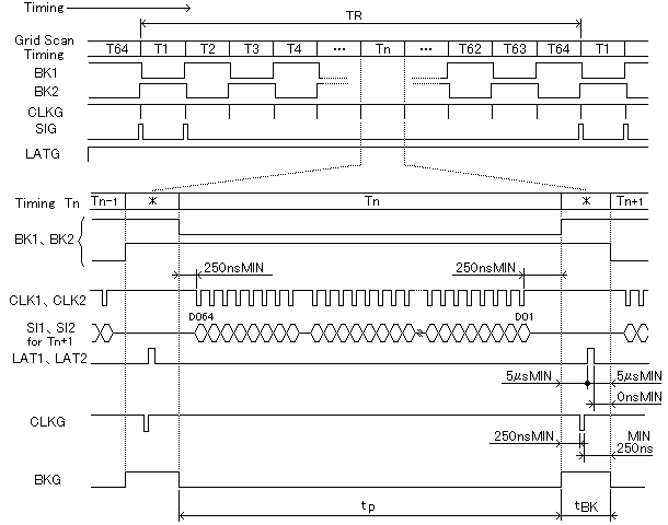
Fig.21 Timing for the Double Anode Drivers of MN12832E
Chip in Glass VFD (BD-VFD)
-
Operation and Structure
-
Power Supply
-
CIG VFD Interfacing
-
Control Procedure
-
Custom Design Guidance
-
Others