Multiplex Drive
Multiplex Grid-Anode Hybrid Interlace Drive
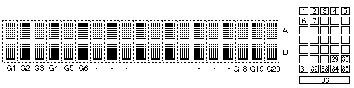
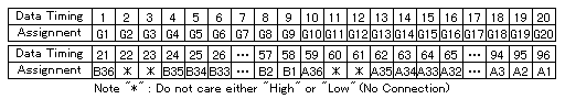
Fig.14 Example of Shift Register Map for the Hybrid Interlace Type
The example display pattern shows a 2 line, 20 character 5x7 dot matrix VFD with underline cursors. The electrodes consist of 20 grids and 2 x 36 anodes which totals 92 driver outputs. Since the driver has 96 outputs, 4 bits * are left unassigned and can be set High or Low.
Bit 1 is sent first (G1) through to bit 96 (A1).
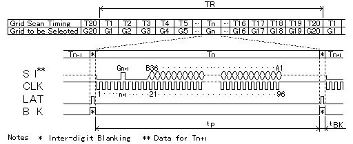
Fig.15 Timing Chart Example for Grid Anode Hybrid Interlace Type
The controlling CPU has the task of sending 20 x 96 bits every refresh cycle (TR). In each of the 20 time slots T1 to T20, the corresponding Grid bit is set High to provide a sequential scan of all the grids.
Anode data bits are also configured for the desired pattern at the enabled grid.
Multiplex Grid-Anode Independent Drive
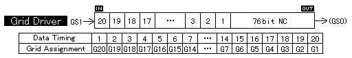
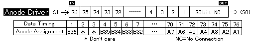
Fig.16 Example of Shift Register Map of the Grid Anode Independent Type
In this example, a 2 line by 20 character 5x7 dot matrix display has 2 separate 96 bit drivers assigned to the 20 grids and the 2x36 anodes.
In this case the grid driver has 76 un-assigned outputs and the anode driver has 24 un-assigned outputs.
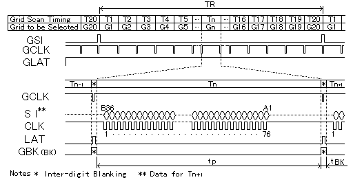
Fig.17 Timing Chart Example for Grid Anode Independent Type
Semi-automatic grid scanning is achieved by setting GS1 to High for the first GCLK pulse then low for the rest of the refresh period. GLAT can be held High to allow the grid shift register data to be directly transferred to the grid outputs.
Time period Tn is expanded to show the 2x36 bits of anode data are clocked in, latched and then displayed in time period Tn+1.
Chip in Glass VFD (BD-VFD)
-
Operation and Structure
-
Power Supply
-
CIG VFD Interfacing
-
Control Procedure
-
Custom Design Guidance
-
Others